Been tracking something interesting the last few days. Started with copper supply forecasts—the kind of dry industry reports that usually don't generate much heat. But this one's different.
The Copper Crunch is Real
Global copper demand is projected to outstrip supply starting 2027, with deficits extending through 2040. The math is straightforward: electrification (EVs, renewable infrastructure, data centers) is consuming copper faster than new mines can spin up. And unlike software, you can't just scale a mine with venture capital and cloud credits.
So the question I've been sitting with: what replaces it?
Nickel as the Obvious Pivot
Nickel is the default answer. It's abundant relative to copper, already used in battery cathodes (NCA/NCM chemistry), and has decent conductivity for certain applications. Some hyperaccumulators—plants that concentrate nickel in their tissues—are being explored for phytomining. Companies are testing nickel alloys for connectors and plating where copper used to dominate.
But here's what caught my attention while reading through the analysis on Grok: nickel isn't really replacing copper in computing infrastructure. It's a stopgap for energy storage and some niche electronics. The real substitution happening—quietly, in parallel—is photonics.
The Photonic Shift Nobody's Pricing In
I wrote about this in From Silicon Valley to Photonic Valley—the Netherlands is pouring €1.1 billion into integrated photonics, China is deploying photonic interconnects to bypass US chip restrictions, and data centers are already migrating to 400G optical modules because copper physically cannot handle the bandwidth AI workloads demand.
Photonics doesn't just reduce copper dependency. It eliminates the bottleneck entirely by moving data at light speed with 0.05-0.2 picojoules per bit—orders of magnitude more efficient than electrical interconnects.
But—and this is the part most coverage misses—photonics has an integration problem. You can't just swap silicon for light-based chips and call it done. The materials don't match. The atomic "lattice constants" are incompatible. Silicon (5.431 Å) and most photonic materials have different crystal structures, which creates defects at the interface.
That's where Indium Phosphide enters the frame.
The 1n40 Code: Indium Phosphide as the Integration Layer
I first came across the "1n40" pattern while exploring semiconductor naming conventions (the 1N4007 diode uses a similar JEDEC prefix). It kept surfacing in my research, and when I dug deeper, Indium Phosphide (InP) was the material at the center.
InP has a lattice constant of 5.864 Å—a precise atomic "blueprint" that makes it the reference standard for integrating photonic components. Materials like Indium Gallium Arsenide (InGaAs) are engineered to lattice-match InP substrates, which is critical for building defect-free photonic integrated circuits.
Here's the practical translation: InP is the "buffer layer" that lets photonics scale commercially.
It's the material that converts electricity into the specific wavelength of infrared light that travels through fiber optic cables (Silica) without signal loss.
It enables lasers, modulators, and detectors to be fabricated on a single chip—"integrated photonics"—which is what makes light-based computing cost-effective at scale.
China's recent progress in photonics, despite US chip restrictions, hinges partly on advances in InP fabrication. The technical challenge isn't just building optical components—it's integrating them without "threading dislocations" (atomic-level cracks) that ruin device performance.
What This Means: Materials Drive Architecture
Zooming out, the pattern is consistent across tech transitions: materials constraints shape system architecture more than we admit.
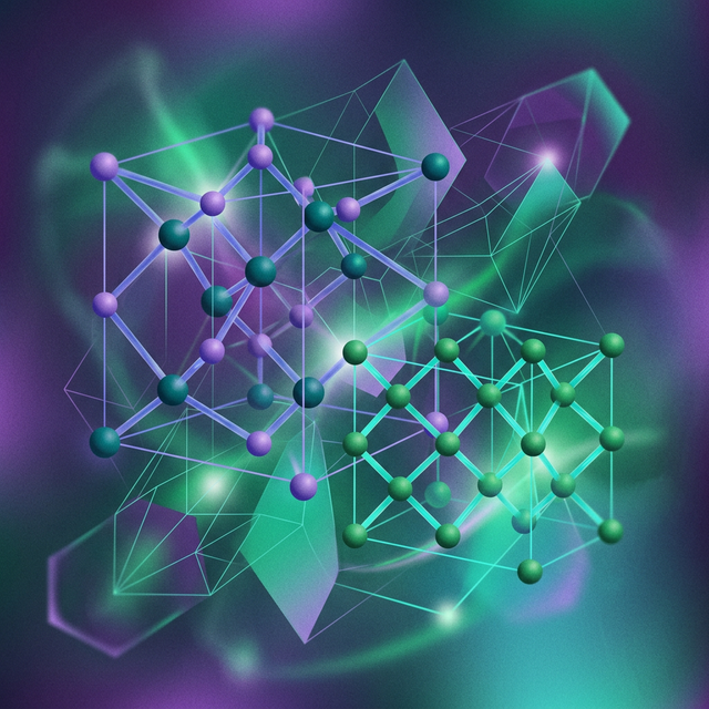
Silicon dominated for decades not because it's theoretically optimal, but because we built an entire manufacturing ecosystem around its 5.431 Å lattice. Now we're hitting physical limits (heat, speed, energy), and the next architecture—photonics—requires different materials with different atomic structures.
Indium Phosphide is rare and expensive compared to silicon, but it's the only material that efficiently generates light at the wavelengths fiber optics need. Trying to build photonic systems without InP is like trying to build electrical systems without copper—you can technically do it, but you're fighting the material's nature.
The nickel pivot, then, isn't just about batteries. It's a signal that the entire materials stack is under pressure. Copper shortages force us to rethink conductivity. Silicon limits force us toward photonics. And photonics forces us toward materials like InP that can "lattice-match" across incompatible systems.
The Integration Problem is the Opportunity
In my Conscious Stack work, I keep coming back to this principle: the constraint is the design. InP's lattice constant isn't a random number—it's the integration tolerance for the entire photonic ecosystem.
When I map this to tech stack design:
Your Anchor tool (using the 5:3:1 rule) is like InP—it defines the "lattice constant" your entire stack must respect.
Tools that don't lattice-match create "threading dislocations"—broken automations, manual re-entry, context-switching friction.
Buffer layers (middleware like Zapier) absorb mismatches temporarily, but they're not foundations. They're the amorphous Silica that flexes between rigid structures.
The companies that dominate the next decade won't just build faster pipes. They'll build compatible faster pipes. Photonics for speed, InP for integration, and—if we're being honest—blockchain for auditability at scale (because moving petabytes per second through AI pipelines without cryptographic provenance is a liability time bomb, but that's a different essay).
What I'm Watching
A few threads I'm tracking:
Fabrication bottlenecks: Smart Photonics (Netherlands) and other foundries are scaling InP wafer production, but capacity is still orders of magnitude below silicon. Who solves manufacturing at scale wins.
China's photonics roadmap: They're not just deploying—they're integrating photonics into data center architecture as a standard, not an experiment. That's a forcing function.
Organic tech speculation: There's fringe research on plants that bioaccumulate nickel and could theoretically inspire bio-engineered photonic materials. Probably a decade out, but worth watching for the "what if."
The InP supply chain: If photonics scales as fast as the investment suggests, Indium becomes a critical material. It's currently a byproduct of zinc mining. That dependency is a geopolitical pressure point.
The Prediction
Copper shortages will accelerate nickel adoption in batteries and niche electronics, but the bigger shift is photonics bypassing the metal bottleneck entirely. And within photonics, Indium Phosphide is the integration layer that makes or breaks commercial viability.
We're not just swapping one material for another. We're transitioning from electron-based to photon-based infrastructure, and that requires fundamentally different atomic architectures. InP is the "lattice" that holds it together.
Still processing the full implications. Not sure we've fully grappled with what it means to rebuild computing infrastructure from the materials layer up. But the movement's real, it's funded, and it's solving actual problems.
What are you seeing in materials science or photonics that I'm missing? Does the InP angle track with what you're observing in the field?
Comments


